


BMBF-Project "MaKiZu - Materialintegration und Kinetik von zuverlässigkeitslimitierenden Degradationsmechanismen in 1D-Elektronik-Systemen"
DCN sucessfully finished project with nanowires
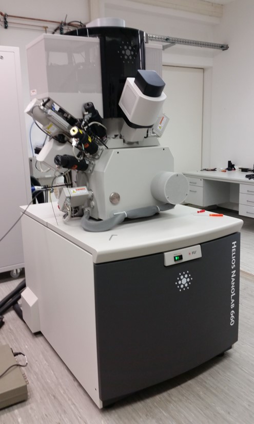
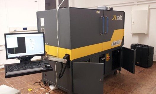
The Dresden Center for Nanoanalysis (DCN) successfully finished a 3-years project to investigate one-dimensional nanowires. The project called "Material integration and kinetics of reliability degradation mechanisms limiting in 1D electronic systems" was funded by the Federal Ministry of Education and Research (BMBF). The DCN team worked in close cooperation with scientists from our partner institute Fraunhofer-Instituts für Keramische Technologien und Systeme Dresden (IKTS). The funding was also used to order both a scanning electron microscope with focusing ion beam and a sub-meter x-ray tomograph.
A scanning electron microscope with a focused ion beam (SEM/FIB) and a sub-micrometer X-ray tomograph were purchased. Additionally needed major equipment - including a nano X-ray tomograph and a transmission electron microscope – which are available at the TU and the cooperative research institutes, has been used for the research project. The project has been granted with about 3.2 millions of Euros by the Federal Ministry for Education and Research. In October 2013, three staff members - a postdoc, a PhD student and a technician - started their work. The goal was the implementation of an interdisciplinary technology platform in cfaed.
In the project managed by Professor Ehrenfried Zschech, reliability-limiting degradation mechanisms in one-dimensional devices systems has been analyzed in order to establish a basis for process development and quality control of future microelectronic products.
Innovative electronic devices based on one-dimensional nanostructures like silicon nanowires and carbon nanotubes as well as nanoscale sensors has been expected to have a much higher performance than current CMOS devices and sensor systems. Thus, new applications will become possible in the fields of automotive, mechanical engineering, logistics, energy, sensor technology as well as medical engineering and health monitoring. Through close collaboration with innovative companies, the research has been sucessfully oriented toward an industrial use right from the start.
Facts
Funded by the Federal Ministry for Education and Research (BMBF)
Funding period: 01.06.2013-30.11.2016
Funding volume: 3,2 Mio. €
Project manager: Prof. Ehrenfried Zschech
PostDoc: Dr. Markus Löffler
Technician: Alexander Tahn
PhD student: Jin Huang
![]()
FEI Helios NanoLab 650 |
Xradia Versa 520 |
|
|
 |
 |