


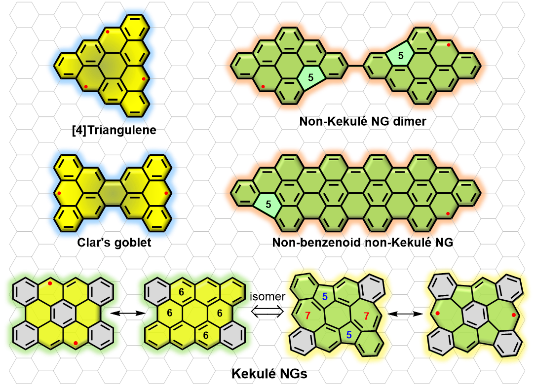
Novel Non-Kekulé and Kekulé Hydrocarbons
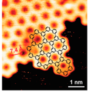
Intense research efforts have been dedicated to inducing magnetism in carbon-based nanomaterials owing to their improved magnetic performance, such as lower spin-orbit couplings and larger spin correlation lengths, than many inorganic materials. Non-Kekulé polycyclic hydrocarbons (PHs) (or nanographenes (NGs)) belong to the class of carbon-rich molecules for which no Kekulé valence structures can be drawn without leaving unpaired electrons, which makes such compounds inherently magnetic and attractive for exploring their fundamental physicochemical properties. Here we are interested in the synthesis of novel non-Kekulé molecules and open-shell Kekulé PHs, which exhibit unique electronic and magnetic properties as well as the potential applications for organic electronics and spintronics.
Graphene Nanoribbons
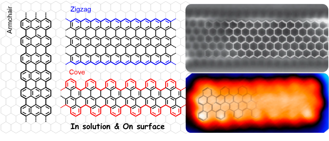
Graphene nanoribbons (GNRs) are considered to be next-generation carbon materials for the fabrication of nanoscale electronic devices owing to their high electrical conductivity and tunable bandgaps. We are particularly interested in synthesizing structurally well-defined GNRs with different topologies through solution-mediated or surface-assisted methods. Programming the shape, width, length, and edge structures of GNRs by the bottom-up organic synthetic methods, allows us to achieve unique insights into their structure-property relationships. Solution processability of GNRs is an important concern for us to readily transfer them on the substrate for reliable device fabrications, hence, synthetic control of GNRs with enhanced solution dispersibility is also our consideration.
Novel Curved Nanographenes
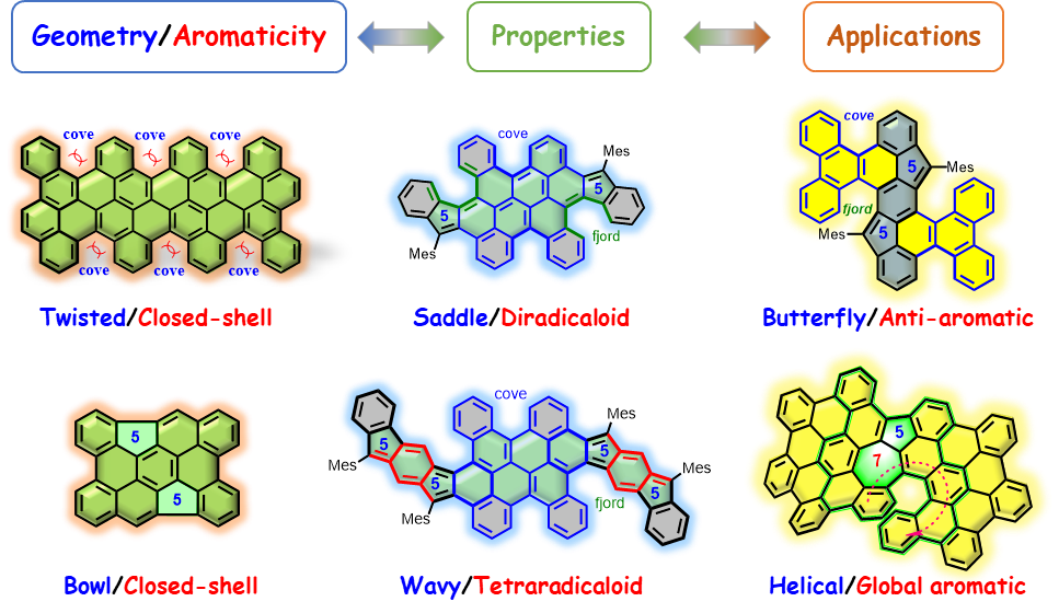
Curved nanographenes have grown to become an important field of research due to their fascinating intermolecular packing, extraordinary chiroptical properties and dynamic behavior resulting from their contorted conformation, which are not shared by the traditional “flatland”. To date, two distinct strategies have been established for the synthesis of curved polycyclic aromatic hydrocarbons (PAHs), including the imposition of non-hexagonal rings and the introduction of steric strain in the molecular skeleton. The increased solubility, novel aromaticity, helicity, chirality, and curvature-dependent opto-electronic properties are key features of this class of PAHs. We are particularly interested in controlling the geometry and the aromaticity of curved π-conjugated systems with the aim of the development of novel functional materials for organic electronics and spintronics.
Heteroatom-doping (isoelectronic) Carbon Nanostructures
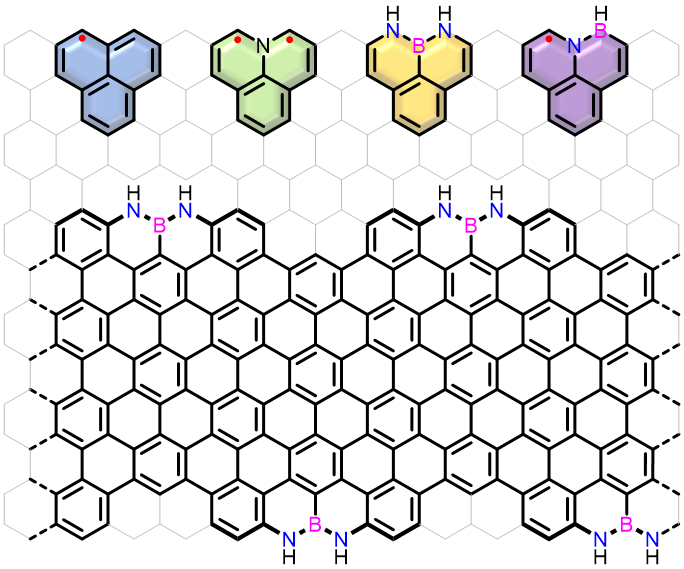
Replacing single or multiple carbon atoms in the sp2-carbon framework by heteroatoms such as nitrogen, boron, oxygen, phosphorous or a combination of them, is an efficient and unique pathway to tune their optoelectronic properties without changing the structural skeleton. Additionally, the stability and aromaticity of the resulting carbon nanostructures can be strongly influenced. We are particularly interested in developing new methodologies to synthesize the isoelectronic carbon nanostructures and explore their new functions for electronics and energy-related fields. The fundamental aspects of chemistry and physics of the heteroatom-doped carbon nanostructures are the core of our interests.
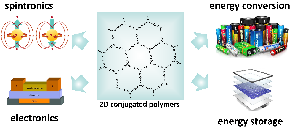
Following on the decades of investigation on the synthetic linear conjugated polymers with notable application potential in organic electronics such as organic field-effect transistors, organic solar cells and organic light-emitting diodes, two-dimensional conjugated polymers (2D CPs) have recently attracted growing research interest as a new generation of organic semiconducting materials. 2D CPs, as represented by graphene and 2D p-conjugated covalent-organic frameworks, are characterized by multi-strands of linear conjugated polymers with in-plane π-conjugation and regular 2D framework structures. The 2D CP subgroup of the Chair of Molecular Functional Materials is geared towards the synthesis of unprecedented 2D conjugated polymers with tailored opto-electronic properties by organic and polymer chemistry. We are focused to establish the rational synthetic methodologies for the solution synthesis of crystalline vinylene- and aryl-linked 2D CPs under controlled reaction conditions, among others. Furthermore, we aim to explore the unprecedented structure-property relationships of 2D CPs based on a variety of characterization methods. We also target at the implementation of these innovative materials into a variety of applications, such as organic electronics, spintronics, energy storage and conversion.
Reaction Methodology
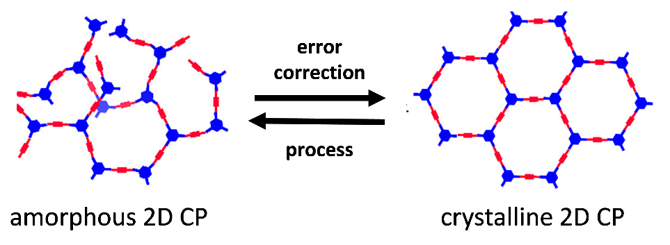
Vinylene-linked 2D CPs have attracted increasing attention in terms of their intrinsic chemical stability and enhanced delocalized electronic structures. However, the synthesis of crystalline vinylene-linked 2D CPs remains challenging, because the C=C bond formation suffers from lower reversibility resulting in kinetically controlled amorphous porous polymers. The crystallinity of the obtained vinylene-linked 2D CP is not high yet, and the size of crystallites is limited to tens of nanometers. To achieve highly crystalline vinylene-linked 2D CPs, we like to gain deep understanding and controlling of the reaction kinetics to facilitate the reversibility, which is essential for achieving highly crystalline vinylene-linked 2D CPs. Other synthetic strategies for the novel 2D conjugated polymers including 2D polythiophene, 2D polypyrrole, etc, are also explored in our group.
Unprecedented 2D CPs
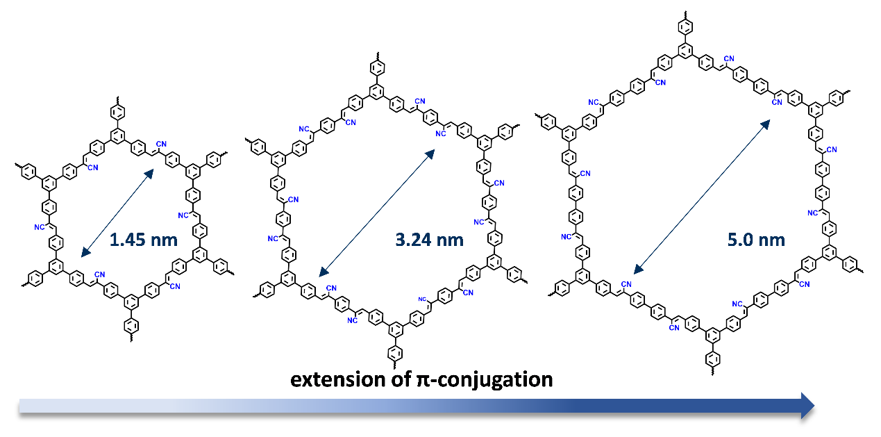
2D CPs have the advantage that the structures or topologies can be easily tailored by the implementation of different building blocks. In particular, the design of the monomers with different sizes, symmetries, substituents and reactive sites dramatically influence the structure and topology of 2D CPs. We are interested in the synthesis of unprecedented 2D CPs with attractive building blocks, topologies or functionalities.
Unique Properties of 2D CPs
Linear conjugated polymers have been well explored for electronic and optoelectronic devices. However, they provide a low charge carrier mobility due to the intermolecular hop of charges. To overcome these limitations, the extension of the π-conjugation into a second dimension provides a plausible solution to increase their mobility. For instance, graphene, which is a prototype 2D CP, demonstrates a high charge mobility of up to 200 0000 cm2V-1s-1. Although graphene has attractive electronic properties, it remains useless as a semiconducting material and thus for possible applications in digital electronics, because of the missing energy gap. In contrast, synthetic 2D CPs with a fully π-conjugated structure provide a well-defined energy-gap, which can be tailored by the organic synthesis. We are interested in the synthesis of highly conjugated 2D CPs with tailored redox- and/or (opto)electronic properties, which can be implemented into a variety of applications, such as electronics, optoelectronics, spintronics, energy storage, etc.
ORGANIC 2D MATERIALS
The discovery of graphene in 2004 has triggered enormous interest in developing chemistry of synthetic two-dimensional materials (2DMs). In this O2D group, we mainly focus on the development of organic 2DMs, which refer to crystalline 2D nanostructures comprising carbon-rich repeated units linked by covalent/noncovalent bonds, including synthetic graphene, 2D polymer (2DP), 2D supramolecular polymer (2DSP), single/few-layer 2D COFs/MOFs, etc. We expect to establish novel chemical/synthetic methodologies toward the controlled synthesis of organic 2DMs and achieve delineation of reliable structure-property relationships and superior physical and chemical performances of organic 2DMs. In this respect, four research areas are involved, including (1) Development of interface-assisted synthesis methodologies; (2) Synthetic 2D polymers/2D COFs; (3) MOFtronics: chemistry of 2D conjugated MOFs and functions for (opto-)electronics, spintronics and energy; (4) Novel van der Waals heterostructures.
Research Area I: Development of Interface-Assisted Synthesis Methodologies
An interface is a flat or curved space (or a phase boundary) between two different matters, or two different phases in one matter. The thickness of the interface space can range from several angstroms to nanometer and even to micrometer size. In our work, we aim to develop interfaces as key roles in “bottom-up” synthesis, which is advantageous for directing the pre-orientation of the molecules or precursors for subsequent 2D polymerization toward organic 2DMs. Typically, the reactions at the interfaces between air−water (or gas−liquid, LB), liquid−liquid, liquid−solid, and gas−solid (or vacuum-solid) are explored for the 2D polymerization by linkage chemistry and the paramount control over the morphology and the structure of organic 2DMs.[1-3] In our latest work, we have established a surfactant-monolayer-assisted interfacial synthesis (SMAIS) method to prepare 2D polymers, like 2D polyimides,[4] 2D polyimines[5] and 2D boronate ester-linked polymers,[6] thus achieving few-layers and micrometer-sized single-crystalline domains.
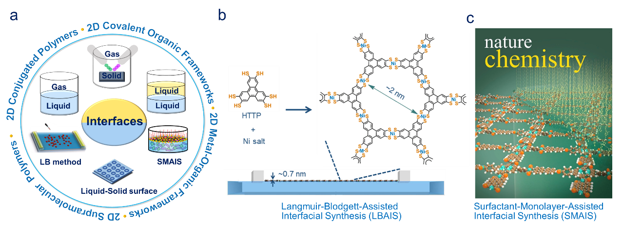
Figure | (a) Schematic illustration of interface-assisted reactions toward organic 2DMs.[1] (b) Langmuir-Blodgett-assisted interfacial synthesis (LBAIS) toward monolayers.[2] (c) Surfactant-monolayer-assisted interfacial synthesis (SMAIS) toward few-layers.[4]
Research Area II: Synthetic 2D polymers/2D COFs
Two-dimensional polymers (2DPs) and their layer-stacked 2D covalent organic frameworks (2D COFs) have emerged as a class of structurally defined organic 2D materials with exotic physical and chemical properties. These porous crystalline polymers generally comprise repeated units linked via covalent bonds with long-range ordering in two distinct directions and have displayed diverse physical and chemical properties for broad functions in (opto-)electronics, spintronics, membrane, catalysis, and energy storage and conversion. Yet, controlled synthesis of 2DP and 2D COF single crystals still remains an immense challenge.
- Dynamic covalent reactions
We aim to explore thermodynamically reversible dynamic covalent reactions (DCRs) for the synthesis of crystalline 2DPs/2D COFs at interfaces and in solution. DCRs allow the atomically precise integration of organic units to create periodic networks with long-range order linked by covalent bonds. A key feature of DCRs is the thermodynamically controlled product distribution at equilibrium. Typical examples of DCRs include the formation of boronate ester, imine, pyrazine, azine, imide, amide and azodioxy bonds. In our recent work, by combining DCRs and SMAIS, we successfully achieved few-layer 2DP single crystals with the domain size up to ~150 μm2.
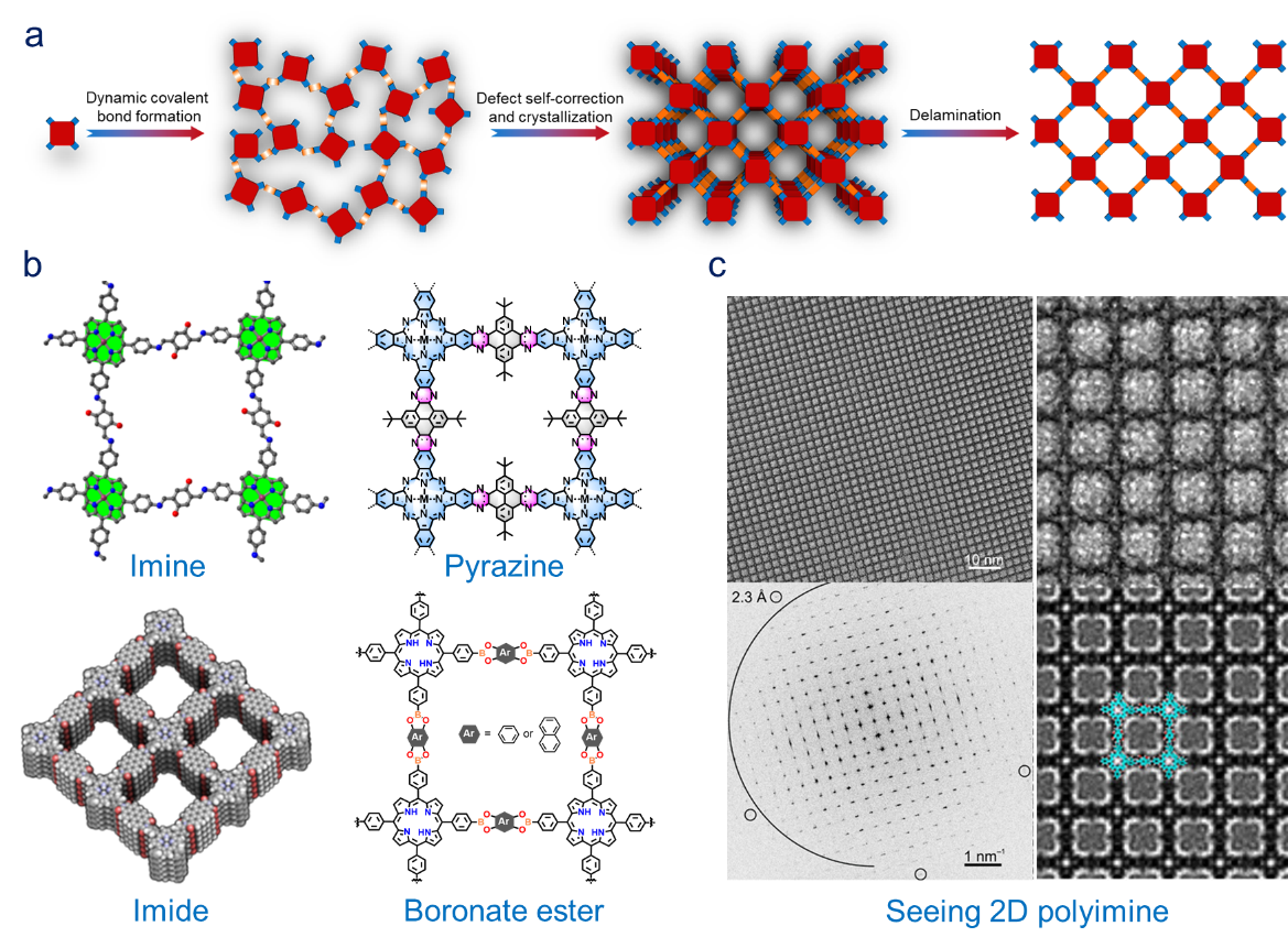
Figure | (a) 2D polymerization under thermodynamic control relying on self-correction after bond formation toward layered crystals and subsequent delamination. (b) Representative 2D polymers/2D COFs based on imine,[5] pyrazine,[7] imide[4] and boronate ester[6] linkages. (c) HRTEM imaging and electronic diffraction of 2D polyimine by SMAIS.[8]
- Irreversible covalent reactions
We aim to explore the utilization of kinetically irreversible covalent reactions (ICRs) for the synthesis of 2DPs and 2D COFs, which is highly attractive but remains challenging. To achieve the long-range order and layered crystals, 2D polymerization will be carried out under kinetic control relying on monomer pre-organization prior to bond formation. Typical ICRs including Knoevenagel,[9] Aldol-type and Horner-Wadsworth-Emmons condensation[10] reactions have been developed for the solvothermal synthesis of vinylene-linked 2D COFs, yielding fully conjugated polymer materials with high chemical and thermal stabilities. On the other hand, structurally-defined conjugated 2DPs can be realized via the on-surface Ullmann coupling under ultrahigh vacuum conditions. Recently, we also performed the oxidation polymerization on water surface by SMAIS and developed wafer-sized, highly crystalline quasi-2D polyaniline thin film,[11] which exhibited a high conductivity up to 160 S/cm.
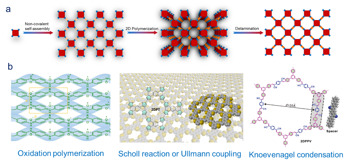
Figure | (a) 2D polymerization under kinetic control relying on monomer pre-organization prior to bond formation toward layered crystals and subsequent delamination. (b) Representative examples: quasi-2D polyaniline via oxidation polymerization,[11] 2D polythiophene via Scholl reaction or Ullmann coupling, and 2D Poly-(phenylenevinylene) via Knoevenagel condensation reaction.[9]
- Functions for electronics, energy and membrane
Synthetic 2D polymers and 2D COFs feature with intrinsic porosity and flexibility as well as tailored electroactivity and photoactivity. In our recent work, upon I2 doping, a phthalocyanine-based pyrazine-linked 2D COF exhibited high conductivity (10-3 S/cm) and record mobility reaching to 22 cm2/(Vs).[12] These unique features enable 2D polymers and 2D COFs broad functions in transistors, sensors, flexible devices, memory devices,[6] membrane separation, osmotic power generators, electro-/photo-catalysis, batteries and supercapacitors.[13]

Figure | Boronate ester based 2D polymer films for neuromorphic memory device.[6]
Research Area III: MOFtronics_chemistry of 2D conjugated MOFs and functions for (opto-)electronics, spintronics and energy
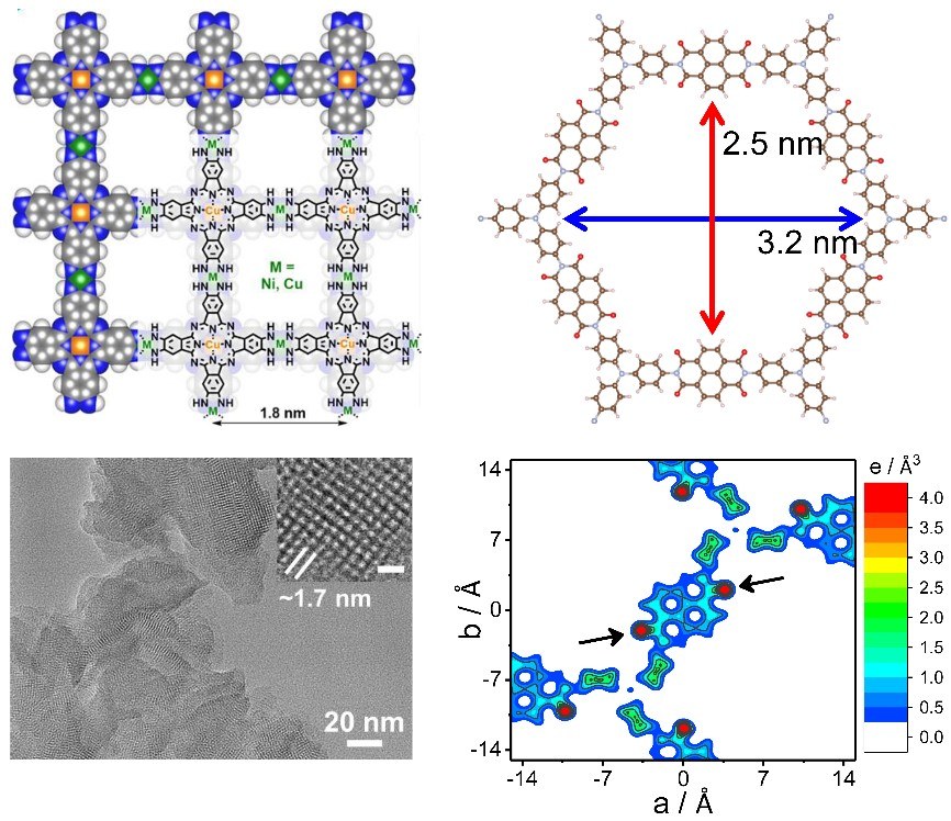
Two-dimensional (2D) π-conjugated metal-organic frameworks (2D c-MOFs) refer to layer-stacked MOFs linked by square-planar complexes with in-plane π-extended conjugation. They have similar structural features to graphite and other van der Waals layer-stacked materials, and in recent years have displayed much higher conductivities (up to 2500 S/cm) than conventional three-dimensional (3D) MOFs (<10-8 S/cm),[14] or demonstrated charge mobility of 220 cm2/Vs with band-like transport.[15] The enormous chemical and structural diversity of ligands and metal ions provides researchers with a playground filled with infinite creative possibilities, allowing design of 2D c-MOFs.[16] Although there are no commercial devices that yet incorporate 2D c-MOF materials, numerous proof-of-concept device demonstrations have appeared, such as transistors, photodetectors,[17] sensing, magnetics,[18,19] and energy storage[13,20,21] and conversion[22,23]. These advances are highly inspiring and demonstrate that 2D c-MOFs are an emergent class of layered electronic materials.
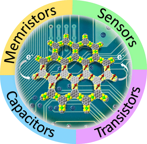
Figure | Schematic illustration of MOFtronics.[14,16]
- Chemistry of 2D conjugated MOFs
To date, around fifteen 2D c-MOFs have been reported based on planar polycyclic aromatic ligands (such as benzene, triphenylene, coronene, phthalocyanine and dibenzo[g,p]chrysene derivatives) with symmetrical functional groups (-OH, -NH2, -SH).[14,16] First of all, we aim to explore the influence of molecular design (type and geometry of ligand, metal) and material structure (redox-activity in linkage, layer stacking and arrangement) on the charge transport properties for 2D c-MOFs. Secondly, another essential question is how to optimize the reaction conditions to pursue high crystallinity.[24] Traditional approaches for controlling crystal growth generally involve varying solvent, concentration, reaction temperature, and time. Nevertheless, these strategies have failed in suppressing the anisotropic growth of a crystal because the in-plane metal-coordination bonds are too strong while the π-π stacking interaction is relatively weak. Thus, the crystal growth is usually dominated by the more reversible π-interaction to yield needle-like morphology with limited crystalline domains parallel to the intralayer direction, or even polycrystalline powders with tiny crystallites (up to hundreds of nanometers in size). Therefore, a rational ligand design will be the first step for establishing highly crystalline sample, thus achieving intrinsic electronic properties. On the other hand, we also explore a variety of synthetic methods to develop 2D c-MOFs, such as solvothermal synthesis, interface-assisted synthesis, on-surface synthesis and surfactant-assisted synthesis as well as CVD synthesis, which render 2D c-MOFs with various morphologies such as bulk crystals, ultra-thin nanosheets (<5 nm), and single-/few-layer films.
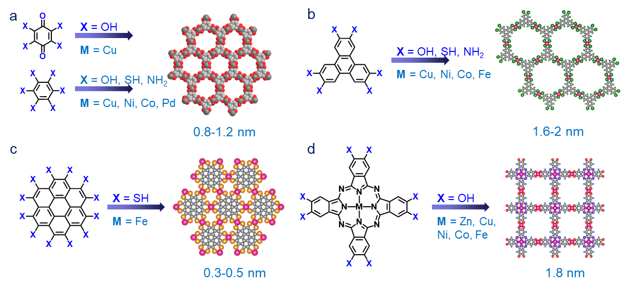
Figure | Representative organic ligands and the relevant 2D c-MOFs with hexagonal and square lattices.
- 2D c-MOFs for (opto-)electronics
The high-conductivity or high-mobility 2D c-MOFs with tunable band structures exhibit promising potential as fascinating electroactive layers for opto-electronic devices. We are particularly interested in defining their intrinsic photo-/electron-transport properties via DC (like time-resolved terahertz spectroscopy) and AC measurements (like 2 probe, Hall effect and Van der Pauw).[15,17] As a consequence, we expect to establish a reliable structure-property relationship and achieve superior device performance for transistors, photodetectors and sensors.
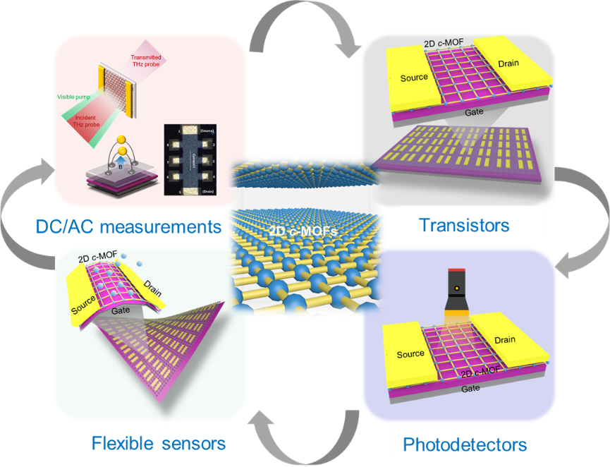
Figure | Schematic illustration of 2D c-MOFs for (opto-)electronics.
- 2D c-MOFs for spintronics
Spintronics, also known as spin transport electronics, has been intensely researched for the next generation of quantum computing and data storage, because spintronics could offer an exciting prospect of combining the semiconductor-based information operation (logic) and magnetic based data storage (memory) into the same device. Historically, spin-related phenomena have been widely studied in inorganic semiconductors; however, the entirely inorganic composition prevents a facile tunability of magnetic and conductive properties due to the lack of both ligand functionalization and structural diversity. In this respect, (semi-)conductive 2D c-MOF hold promise because the magnetic behavior can be tailored at the molecular scale through tuning their building blocks, metal centers (spin carriers) and even filling functional guest molecules or introducing radicals into the porous. For this purpose, we aim at the design and synthesis of 2D c-MOF magnets for spintronics.
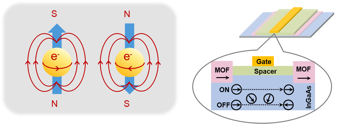
Figure | Schematic illustration of 2D c-MOFs for spintronics.
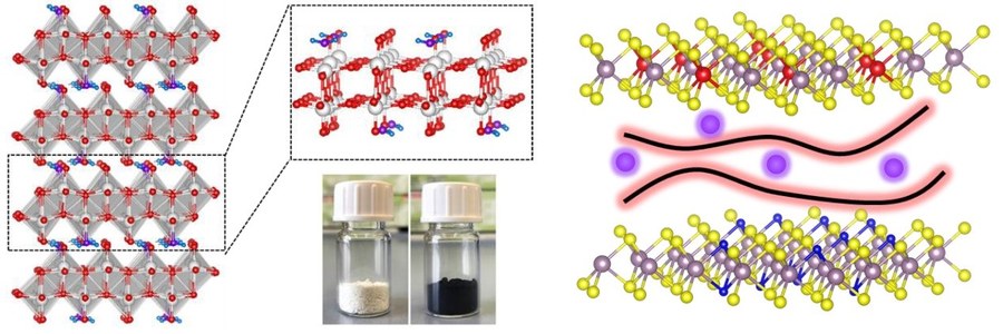
- 2D c-MOFs for electrochemical energy storage
Conductive 2D c-MOFs incorporating redox active units have emerged as a novel class of multifunctional electrode materials for electrochemical energy storage. Metal-ion batteries and supercapacitors represent two major energy storage devices. Benefiting from the intrinsically conductive and porous properties, 2D c-MOFs have shown excellent performance in metal-ion batteries[21] and supercapacitors,[20] which could function as the power sources for the above mentioned MOFtronics.
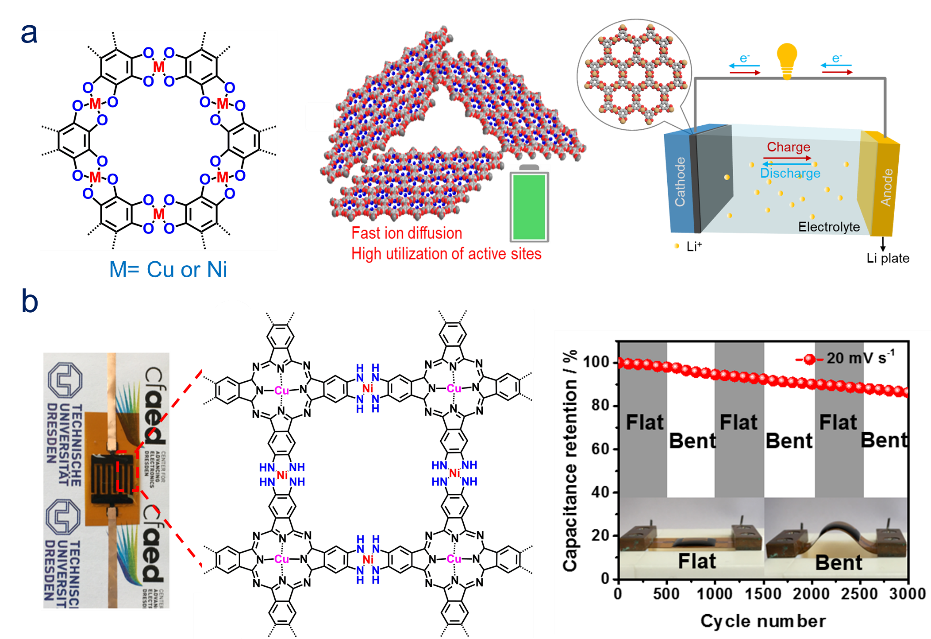
Figure | Schematic illustration of 2D c-MOFs for electrochemical energy storage. (a) Li-ion battery.[21] (b) Flexible microsupercapacitor.[20]
- 2D c-MOFs for electrochemical energy conversion
The exploration of effective electrocatalysts has advanced the development of electrochemical energy storage and conversion technologies, such as fuel cells, water splitting, and metal–air batteries. 2D c-MOFs are highly attractive catalytic systems due to the uniquely combining homogenous and heterogeneous features: 1) the incorporation of well-defined and highly active sites into a defined and stable scaffold ensures excellent catalytic activity and selectivity; 2) the porous metrics allow for sufficient and controllable mass transfer to and from the embedded active sites; 3) the molecularly defined catalytic environment around the active site allows for tuning the catalytic reaction by modifying the scaffold and facilitates deriving fundamental understanding of catalytic mechanism. To achieve high catalytic performance, our research focus on the design and synthesis of novel 2D c-MOFs with well-defined active sites and porous structures for mass transfer.
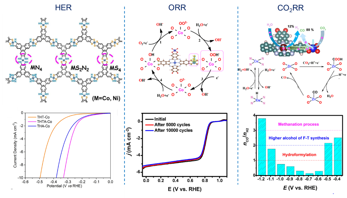
Figure | Schematic illustration of 2D c-MOFs for electrochemical energy conversion, including HER,[2,24] ORR22 and CO2RR.[23]
Research Area IV: Novel van der Waals heterostructures
Two-dimensional (2D) van der Waals heterostructures (vdWHs) are generated by integration of 2D materials with dangling-bond-free surfaces through the weak interlayer vdW interaction along the vertical direction. In recent years, 2D vdWHs have attracted increasing attentions due to the diverse components and novel functions in photodiodes, phototransistors, tunneling devices and memory devices. Through surface reconstruction and proximity effects between the neighboring layers, the optoelectrical properties of vdWHs can be tailored, thus tuning carrier density, improving electron-hole separation and accelerating charge transfer. In our work, we aim to establish bottom-up chemical methodologies toward the synthesis of organic 2DM based vdWHs, control the chemical synthesis for high-quality vdWH interface with atomic precision, and elucidate the structure and physical/chemical property of the synthetic vdWHs.
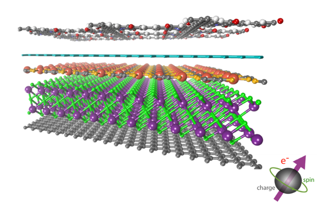
Figure | Schematic illustration of organic 2DM based vdWHs.
References:
- Rev. 2018, 118, 6189-6235.
- Chem. Int. Ed. 2015, 54, 12058-12063.
- Commun. 2016, 7, 13461.
- Chem. 2019, 11, 994-1000.
- Chem. Int. Ed. 2019, 59, 6028-6036.
- Chem. Int. Ed. 2020, 59, 8218-8224.
- Am. Chem. Soc. 2019, 141, 16810-16816.
- Adv. 2020, 6, eabb5976.
- Chem. 2016, 7, 4176.
- Chem. Int. Ed. 2020, 59, 23260-23625.
- Commun. 2019, 10, 4225.
- Am. Chem. Soc. 2020, 142, 21622-21627.
- Am. Chem. Soc. 2020, 142, 12903-12915.
- Rev. 2020, 120, 8581-8640.
- Mater. 2018, 17, 1027-1032.
- Soc. Rev. 2021, DOI: 10.1039/D0CS01160F.
- Mater. 2020, 32, 1907063.
- Commun. 2018, 9, 2637.
- Commun. 2019, 10, 3260.
- Funct. Mater. 2020, 30, 2002664.
- Sci. 2020, 11, 7665-7671.
- Chem. Int. Ed. 2019, 58, 10677-10682.
- Commun. 2020, 11, 1409.
- Mater. 2021, 20, 122-123.
- Eur. J. 2017, 23, 2255-2260.
INTERFACIAL SYNTHESIS
So far, solution synthesis of 2D materials met with limited success due to the decreasing solubility of the synthesized compound with the increase of each single repeating unit, which leads to its precipitation and limits its lateral size to several nanometers. Moreover, in solution there is no driving force enabling the synthesized compounds to grow into a 2D geometry. To overcome this disadvantage, we use interfaces as reaction places where the ordering of monomers and the polymerization into large-area 2D materials occurs simultaneously.
 [
[
HETEROSTRUCTURES FOR OPTOELECTRONICS
The success of graphene has triggered the birth of other two-dimensional sheets with a thickness of one atom or molecule. Reassembly of these sheets with graphene into three-dimensional stacks with one atom-/molecule-layer precision has led to the emergence of graphene van-der-Waals heterostructures as a new class of materials. The structures provide enormous opportunities to combine the properties of all individual components, to explore their synergic effects, and thus to tailor them for a specific application. We focus on the generation of graphene heterostructures with conjugated 2D materials for flexible optoelectronics.
NOVEL POROUS POLYMERS
Porous polymers with controllable porosity at the atomic scale have attracted tremendous attention due to their easy-controlled porous channels, availability of various building blocks, light weight, prominent physicochemical properties and numerous potential applications in sensing, gas storage and separation, energy storage and conversion, etc. We are focusing on the design and synthesis of novel porous polymers with dimensionality control (including conjugated microporous polymers, hyper-cross-linked porous polymers, covalent triazine-based frameworks), which will open a new door to emerging applications.
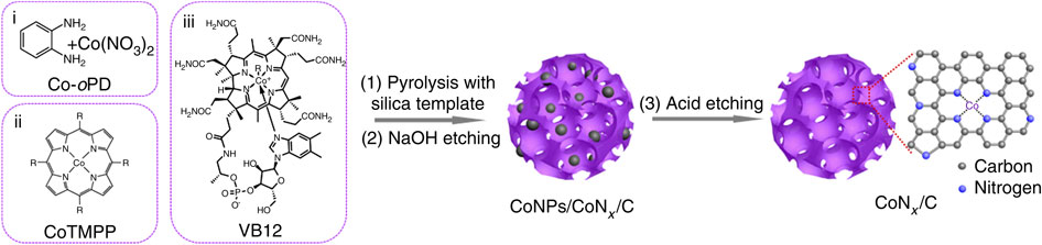
POROUS CARBON MATERIALS
Porous carbons possess controllable and hierarchical pore sizes (micropore, mesopore, and macropore) with different pore structures (order and disorder) showing a variety of applications for energy storage and conversion. Novel controlled synthetic protocols and new functions as well as the understanding of mechanisms become essential for porous carbon materials.
POROUS CARBON-HYBRID SYSTEMS
Due to the high surface area and good conductivity of porous carbons, integration of porous carbons with functional inorganic nanomaterials becomes one promising approach to build up new hybrid materials for energy applications with enhanced performance.
GRAPHENE-BASED HYBRIDS
The assembly of graphene and its derivatives with inorganic species opens up an exciting new field in design and construction of composites with hierarchical superstructures. Until now, diverse synthetic protocols have been developed for hybridization of graphene with a series of different inorganic substances including transition metal nanoparticles/nanosheets, transition metal oxides/sulfides/phosphides. Our focus is the development of 2D hybrid materials with sandwich-like morphology and hierarchical macroporous structures for applications in energy storage and conversion.
Next-generation Energy Materials
- Novel Carbon Nanostructures
Novel carbon materials with tailor-made structures (e.g., topological defect, porosity, dopant, morphology) are of significant interest for a variety of energy-related applications. We are seeking for the development of novel structurally well-defined carbon nanostructures. The fundamental understanding of carbon growth mechanism, and new physical/chemical/electrochemical properties will be explored in the context of our research.

- 2D Redox-Active Carbon-Rich Frameworks
2D carbon-rich frameworks (including carbon-conjugated metal-organic frameworks (MOFs) and covalent organic frameworks (COFs)) have emerged as a group of intelligent multi-functional materials, owing to the designable topologies at the molecular level, regular porosities, and large specific surface areas. These materials offer great opportunities to design and synthesize new energy storage electrodes by organizing redox-active monomers into the periodic framework structures. We are highly interested in the design and synthesis of new framework molecules, as well as the investigation of these molecules for the next-generation energy storage technologies.
- 2D Materials & Van der Waals Heterostructures
The large family of atomically thin 2D materials (e.g., Graphene, Phosphorene, MXenes, TMDs, 2D organic materials) collectively covers a very broad range of chemical and physical properties. Van der Waals interaction between distinct 2D materials shows considerable compatibility, allowing the flexible assembly of 2D heterostructures that can synergize each building block's desirable properties. We are particularly interested in developing controllable synthetic routes, surface/defect chemistry control, unique/exceptional physicochemical properties, and energy applications of novel 2D materials and their heterostructures.
Energy Storage
- Supercapacitors and Hybrid-Ion Capacitors
Supercapacitors, which are power-featured energy storage devices, deliver a power density that is one order of magnitude larger than that of lithium-ion batteries. Hybrid-ion capacitors represent one type of emerging energy storage devices, which are made up of a battery-type electrode and a capacitor-type electrode. To achieve high-performance supercapacitor/hybrid-ion capacitor devices, we aim at fabricating thin-film electrodes with large accessible electrochemically activated surfaces, high electrical conductivity, and an elaborate device structure with efficient ion diffusion pathways.

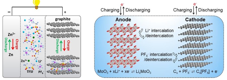
- Dual-Ion Batteries
Anion-storage chemistry provides the possibility to enable battery cathodes with high potential windows (e.g., anion-intercalation graphite with an average discharge potential of > 4.5 V vs. Li+/Li). It opens up new application opportunities for constructing plenty of dual-ion batteries (DIBs), which significantly contrast with the conventional ‘rocking-chair’ Li-ion batteries. We are interested in the development of new anion-storage materials, rational electrolyte preparation, and novel dual-ion battery configuration design.
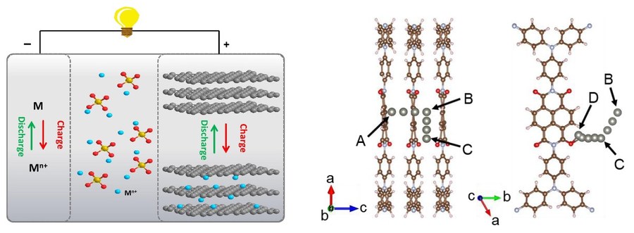
- Multi-Valent Metal-Ion Batteries
Multivalent metal-ion chemistry offers feasible pathways to develop next-generation energy storage technologies with higher energy density, better safety, and lower cost, as the corresponding metals (e.g., Zn, Mg, Al) can be directly used as ideal multielectron-redox anodes. The main challenge of multivalent metal-ion batteries lies in the large difficulty of multivalent metal ions to be stored in convention battery materials, due to the large ionic size and strong repulsive intercalation with host materials. Our research efforts focus on developing high-performance cathode materials for accommodating multivalent metal ions, innovative approaches to alleviate the sluggish ion-storage kinetics, and construction of high-performance battery devices.
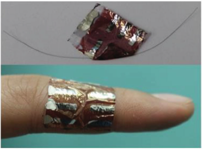
- Functional Devices & Smart Integration
The development of many cutting-edge technologies (e.g., wearable/implantable healthcare devices, environmental monitoring, internet of things) triggers the development of modern electronics towards miniaturized, portable, multi-functional, and highly integrated device systems. High demand for power sources with the same features is imposed, as traditional energy storage devices (e.g., supercapacitors and batteries) may not be of suitable choices. In this regard, we are highly interested in developing miniaturized energy storage devices (micro-supercapacitors and micro-batteries), introducing multi-functionalities into energy storage devices (e.g., mechanically flexibility/stretchability, sensing functions, stimulus-responsive functions), and constructing highly integrated self-powered energy systems.
Energy Conversion
- Electrocatalytic Oxygen Reactions (Metal-Air Batteries, Fuel Cells)
The increasing energy crisis and environmental pollution require innovative solutions for the use of renewable energies. Electrocatalytic oxygen reactions (OER, ORR) are the vital process for next-generation electrochemical energy storage and conversion technologies, e.g., metal-air batteries and fuel cells. Due to their earth-abundance and unique physicochemical properties, carbon-rich nanomaterials can serve as novel materials and electrodes for catalyzing the sluggish oxygen reaction kinetics. In order to achieve high catalytic performance in energy storage and conversion systems, we primarily focus on synthesizing novel carbon-based catalysts with improved intrinsic activity and favorable porous structures for mass transport.

- Photoelectrochemical Water Splitting
Due to the high energy density and clean combustion product, hydrogen (H2) has been universally proposed as a promising energy carrier for future energy conversion and storage devices. Conjugated polymers, featuring tunable band gaps/positions and tailored active centers at the molecular level, are attractive photoelectrode materials for energy conversion. Developing conjugated polymers with small bandgaps, high separation capability of photoinduced holes and electrons, and highly active catalytic centers, provides a promising pathway for photoelectrochemical hydrogen/oxygen evolution reactions.
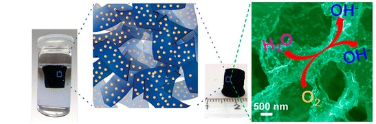
- Nanofluidic Osmotic Power Generation
The osmotic energy between river water and seawater, also known as salinity gradient energy or blue energy, has been identified as promising clean, renewable, and non-intermittent sources of energy. Currently, the industrial utilization of such worldwide energy is mainly limited by the low performance of the commercial ion-exchange membrane. The unique electrolyte transport phenomena in the 2D nanofluidic channel system open a new avenue to harvest osmotic energy. We primarily focus on the design and construction of novel nanofluidic membranes based on synthetic 2D materials, investigation of the ion transport behaviour, and exploration of their application in osmotic power generation.
Research Area I: Emerging Two Dimensional Materials
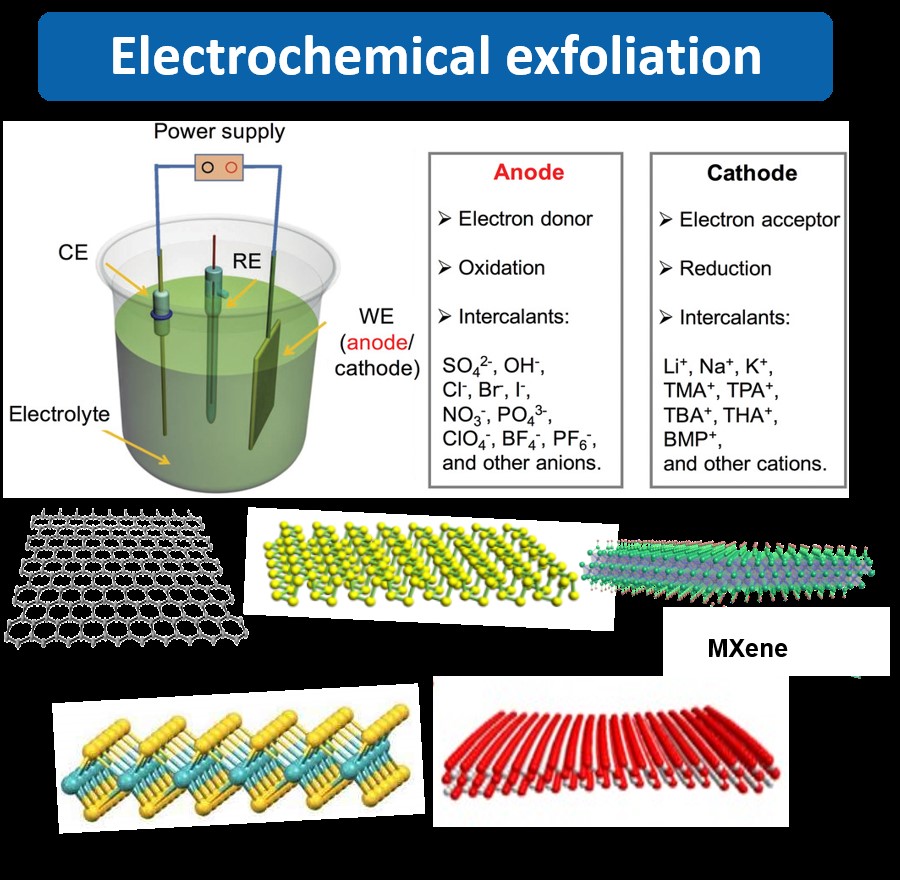
- Electrochemical and Chemical Exfoliation
2D materials are important building blocks for the next generation of electronic, optoelectronic and energy-related devices due to their excellent chemical and physical properties. To this end, scalable synthesis of 2D materials with high purity and specific functionalities represents a key to advancing fundamental studies and industrial applications. Among different synthetic protocols, electrochemical exfoliation of layered materials is a promising approach that offers high yield, remarkable efficiency, low cost, simple instrumentation, and excellent up‐scalability. Remarkably, playing with controlled electrochemistry enables functionalization and tunable material properties and increases the material diversities from graphene to a broad spectrum of 2D semiconductors. In our group, we explore the controlled synthesis, fundamental physical/chemical properties as well as applications of emerging 2D materials such as black phosphorous, indium(III) selenide, MXene, and transition metal dichalcogenides via electrochemical and chemical exfoliation. We aim to establish roubust electro-chemical exfoliation methodologies for the in-situ functionalization, enlabling the enhanced processability and functionaliaty of 2D materials.
Selected Publications:
1- A Delamination Strategy for Thinly Layered Defect-Free High-Mobility Black Phosphorus Flakes. Angew. Chem. Int. Ed. 2018, 57 (17), 4677-4681
2- Fluoride-Free Synthesis of Two-Dimensional Titanium Carbide (MXene) Using A Binary Aqueous System. Angew. Chem. Int. Ed. 2018, 130 (47), 15717-15721.
3- Ultrafast Electrochemical Synthesis of Defect-Free In2Se3 Flakes for Large-Area Optoelectronics. Adv. Mater. 2020, 32 (8), 1907244.
4- Emerging 2D Materials Produced via Electrochemistry. Adv. Mater. 2020, 32 (10), 1907857
Patent and patent applications:
1- Two-dimensional carbon materials prepared by electrochemical exfoliation, WO2015158711A1
2- Method for producing a layered (semi-)conductive material, EP3153605B1, WO2017050689A1
3- Method for the synthesis of MXenes, MXene nanosheets and their use. EP20191753.1
- Functionalization of 2D materials
Most of 2D materials such as transition metal dichalcogenides, 2D metals, transition metal carbides/nitrides suffer from environmental stability. On the other hand, their physical properties, such as bandgaps and charge carrier mobilities, require to be tailored in order to fulfill the targeted applications. In our group, we are using different chemical functionalization strategies to achieve tunable physical properties of 2D materials. Moreover, we aim to develop 2D materials-based inks for large-area fabrication of electronic, optoelectronic and energy-storage devices.
Selected publications:
- Electrochemically Exfoliated High-Quality 2H-MoS2 for Multiflake Thin Film Flexible Biosensors. Small 2019, 15 (23), 1901265.
- Efficient Coupling of Nanoparticles to Electrochemically Exfoliated Graphene. J. Am. Chem. Soc 2015, 137 (16), 5576-5581.
- Alternating Stacked Graphene-Conducting Polymer Compact Films with Ultrahigh Areal and Volumetric Capacitances for High-Energy Micro-Supercapacitors. Adv. Mater. 2015, 27 (27), 4054-4061.
Patent and patent applications:
Process for the preparation of a functionalized semiconductor or conductor material and its use, DE102017223892A1, WO2019129573A2
Research Area II: 2D materials inks and printable devices
- Large-scale production and processability
The first step towards commercialization and industrialization of 2D materials in different areas such as electronics and energy harnessing is to achieve reliable large-scale production and processability of these materials. For this purpose, we have developed a continuous flow process technique for the electrochemical exfoliation of 2D materials. On the other hand, by in-situ functionalization of 2D materials during the the exfoliation process, we can improve the processability of these materials for various applications.
- Printing technologies
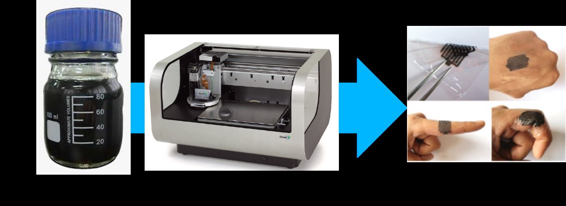
The next step towards real practice is the fabrication of 2D materials with the state-of-the-art printing technologies, which could be further adapted into roll-to-roll processes. To this end, we develop functional inks and pastes for different printing technologies like inkjet printing for the fabrication of different energy and electronic devices such as flexible micro-supercapacitors.
Research Area III: Environmental 2D based foam, coating, and composites
We are developing 2D material based foams, composites, and coatings for environmental applications such as water/air purification, anticorrosion coating, and thermal management. In this regard, we collaborate with top European industries such as BASF, Lufthansa Technik, Barpimo, Polymem, and Tecnalia. Together with Barpimo, we are developing graphene-based waterborne anticorrosion coating paints for automotive industries. In another project with Lufthansa Technik, we are developing self-cleaning graphene-based foams for aircraft's air filtration system. In collaboration with our colleagues in Kiel University and Tecnalia, we are developing different 2D material based foams for desalination technologies for the water purification.
Research Area IV: Development of Energy Storage Devices
With the rapid development of power-demanding smart devices such as wearable electronics and the Internet of Things (IoT), functional energy sources with high energy and power densities, operational safety, long-term stability, in addition to mechanical flexibility, lightweight, thin thickness, and low cost are in urgent need. Therein, we are developing thin and flexible energy storage devices such as batteries and supercapacitors for wearable applications. Within this area, we collaborate with different industries in the fields of energy, wearable electronics, and smart cloth/textiles. For example, we are collaborating with InteractiveWear AG and E-COOLINE, who are active in the area of wearable electronics and thermo-regulator clothes, respectively. We are developing a power system based on flexible graphene supercapacitors to power up the environmental sensors (temperature, humidity, and barometric pressure sensors) within a thermo-regulator jacket.
Patent and Patent applications:
- Bismut-Ionen-Akkumulator. DE 102020101890.8.