Research
CNT transistor platform and advanced technologies for high frequency FETs
In the laboratories of TU Chemnitz and Fraunhofer ENAS we develop and investigate emerging transistor technologies using regular assembled semiconducting CNTs as channel material. A nanotechnology platform was established which enables transistor-based prototype applications on the wafer-level. On this basis we do applied research on nanoelectronics, biological-/chemical-/mechanical sensors as well as integrated devices
One of the core topics of cfaed has been CNT-based high frequency field-effect transistors for future analog transceiver electronics. This technology prospects highly linear FET characteristics and has the potential to exceed GaAs technology in terms of energy consumption and integration capabilities. Meanwhile the technology at TU Chemnitz has reached the 4th technology generation for HFFETs with 280 nm FET channels and 16 GHz fT on 200 mm wafer level. Recently we have completed a study on device geometry [ACS Appl. Mater. Interfaces 2020, 12, 24, 27461 (2020)]. While most studies so far have concentrated on symmetrical top-gated FET devices, we investigated bottom gated asymmetric FET architectures and the influence of their device geometry on the HF performance. Ongoing R&D concentrates on HF circuitry and reliable fabrication technologies for application in the frequency range 5 to 100 GHz.
Wafer-level nanotechnology platform
Advanced technology for integrated sensors
The intrinsic giant piezoresistive effect and mechanical properties of CNTs are predestined to be applied in advanced tactile sensorics, nanoresonators for molecular sensing or highly miniaturized condition monitoring. While this effect is theoretical well understood there is a lack of scalable technological solutions addressing persisting challenges from e.g. chirality distribution of nanotubes, electro/mechanical contact and heterogeneous integration.
In this frame, we recently presented a deep study on MEMS integrated CNT piezoresistors showing more than 3 times higher sensitivity as silicon strain gauges [Sensors and Actuators A: 295, 15, 288 (2019)]. We exposed highly sensitive operation regimes pushing device performance to 150 %, utilized by modifying the CNT-metal Schottky barrier width via drain-induced barrier lowering.
Ongoing research is concentrating new device concepts and technologies as well as combination of various sensors with systems.
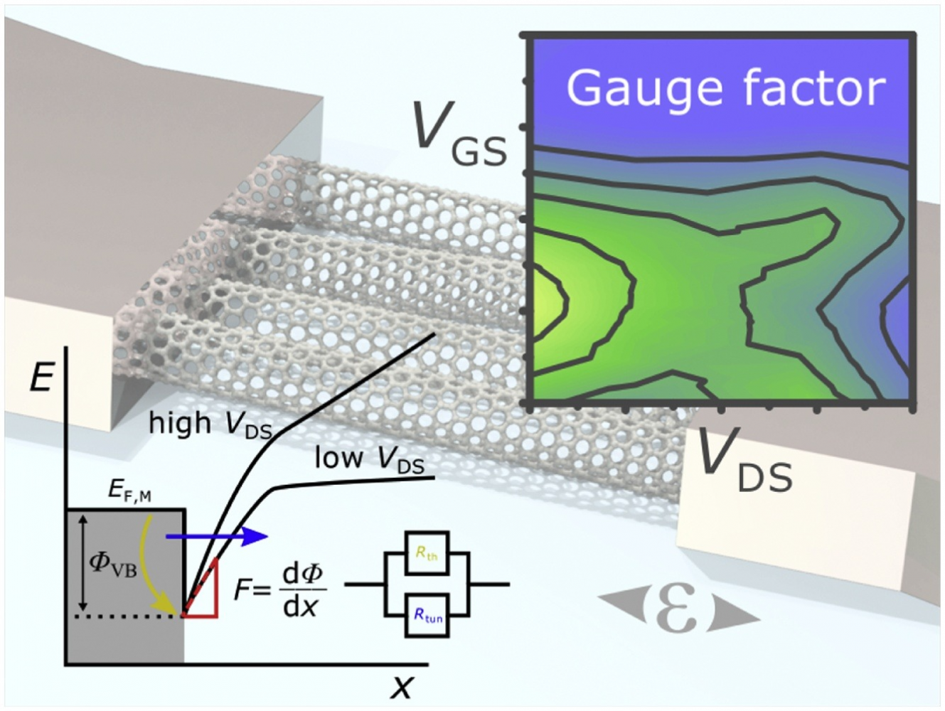
Tuning the sensitivity of giant piezoresistors
Heterogeneous integration of nanodevices into systems
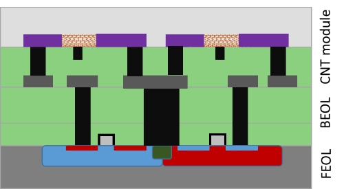
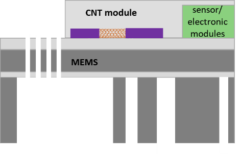
An inevitable evolutionary step for nanodevice technology is the combination with peripheral or any functional environment such as circuitries, energy management, signal processing or System-on-a-Chip. This task involves huge challenges on microtechnological processing and compatibility with typical device technologies. In this frame, we develop heterogeneous technologies for integration of nanomaterials such as CNT-based sensors in MEMS, MOEMS or ASICs.
Exemplarily, in the BMBF funded project SmartStar we are a core technological partner for a new concept aiming to increase the functional safety of electronic systems in autonomous vehicles. Therefore, an integrated condition monitoring is under development. We develop a modular technology for the integration of miniaturized strain-field sensors based on Carbon Nanotubes directly on customized 200 mm ASIC wafers. Along with this project, we push forward advanced technologies for wafer-level processing, control of nanodevice properties, and packaging.
|
Fusion of ASIC- and CNT- technology |
Orchestration of different technology modules on wafer-level |